KORVUS TECHNOLOGY

Thin Film Thickness: Measurement, Importance, and Control

In thin film technology, thickness measurements are a fundamental property of the form and function of the deposited film. Manufacturers must be able to measure and control the thin film thickness for use in a variety of specific capacities.

Techniques to apply thin films to a substrate surface within a particular thickness range include physical vapour deposition (PVD coating), such as e-beam evaporation, and chemical vapour deposition (CVD coating), such as plasma-enhanced deposition. Each offers different levels of control and surface morphology for the film material.

1

The Importance of Thin Film Thickness

The properties of a material’s performance are closely linked to the film thickness measurements. The thickness of the material application can affect its thermal, electrical, mechanical, and optical properties. The type of thin film deposition system impacts the final material thickness measurements, so it’s important to select the right deposition system for the application.

Impacts on Performance and Functionality

1

So how do thin film thickness measurements affect the performance of thin films?

The thickness of thin films is one aspect of many that impart properties to the material.

Optical coatings, superlattice structures for quantum phenomena, tribological coatings, and other bulk substrate coatings target different thicknesses and structural properties during thin film deposition. The thin film properties of each can vary with the thickness compared to the application method of monolayer, nanoscale, multilayer, and superlattice deposition.

By applying thin films in individual layers, you can affect the properties of your materials. This can include hard coatings, anti-reflective coatings, conductive coatings, and coatings to reduce friction and corrosion, along with stacked film coatings used in research such as Bragg stacks. 

How Do You Determine the Thickness of a Thin Film?

When most film coatings are only up to a few nanometres thick, how is thin film thickness measured? Various techniques exist to measure a thin layer of material film over a bulk form, including X-ray reflectivity, stylus profilometry, interferometry, scanning electron microscopy, energy dispersive spectroscopy, ellipsometry, and other techniques. Some of these techniques are destructive, while others are non-destructive.

Non-Destructive Techniques

When considering your method selection, non-destructive techniques and tools include:

Ellipsometry for a wide variety of materials on a smooth material that will reflect light to measure the refractive index (RI) and extinction coefficient, often used for semiconductor devices and electronics

Reflectometry for single or multilayer thin films that will reflect light in a spectrum to determine thickness and RI

X-ray reflectivity (XRR) for multi-layered thin films to measure thicknesses of up to 100 nm

Scanning electron microscopy (SEM) to measure semiconducting films with a thickness range between 100 nm to 100 μm

Transmission electron microscopy (TEM) to measure either conducting or semiconducting thin films in single or multilayer coatings and thickness measurements up to 100 nm

Destructive Techniques

Other techniques require masking on the surface of the bulk material or using cutting tools to remove portions of the film and bulk materials so that you can measure the thickness of the coating.

Two common destructive measurement techniques are stylus profilometry and interferometry.

In both methods, you must have a uniform film application to ensure accuracy in measuring film thickness. Additionally, interferometry requires the surface to be highly reflective to accurately measure the interference fringes.

These techniques are mainly used to calibrate a process to ensure that the films your process is producing is suitable for your application.

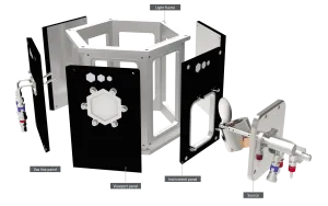
Techniques for Controlling Thin Film Thickness in Deposition Processes

Whether applying decorative coatings or more advanced materials for optical instruments, integrated circuits, or thin film batteries, several application techniques are available to manage the application thickness for thin films.

Pre-Deposition Controls

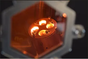
Chemical vapour deposition (CVD) methods include low pressure deposition, plasma-enhanced deposition, and atomic layer deposition. Physical vapour deposition (PVD) methods include thermal evaporation deposition and sputtering deposition.

Sputtering

Before applying thin films using either chemical deposition or physical deposition, you can test your settings using a quartz crystal microbalance (QCM). Coating and monitoring the crystalline structure of a piece of quartz oscillator crystal can allow you to take specific measurements for evaporation deposition processes.

This works through the calibration of the QCM for your system’s geometry and then inputting the necessary tooling factor. The QCM will then read a frequency that will change depending on the deposition onto the crystal – in turn, giving you your deposition onto your sample.

Using chemical deposition, you can avoid differences in thickness that can come from spin coating or some physical deposition methods.

In-Situ Deposition Controls

When it comes time for the deposition method selection of a thin film on a material, you must consider factors like surface roughness and elemental composition of the film and the substrate to decide how to control thin film thickness.

Whether you want to use pulsed laser deposition for a growth mode at the atomic level or a vacuum thermal evaporation technique, different in-situ deposition control tools are available.

Plasma emissions monitoring uses plasmonic devices in magnetron sputtering deposition to measure the deposition of oxide and nitride films on pure metal substrates.

An optical monitoring system (OMS) is a process that allows real-time monitoring of each layer’s thickness when applying multilayer thin films. It can monitor a substrate directly or use a reflection or light transmission through a witness chip to monitor the surface diffusion indirectly.

Post-Deposition Controls

You may need to test samples of coated parts to ensure accurate thin film thickness during application. How thick are thin films? For example, molecular beam epitaxy should leave an ultra-thin film that is only one molecule thick for each layer. If you made three layers, then depending on the original surface roughness of the substrate, the thin films applied should be approximately three molecules thick.

Post-deposition controls use surface science to determine if the elemental composition of the thin film reached the appropriate thickness and didn’t exceed the required parameters for your coating job.

What’s Best for You?

TAU

Korvus Technology uses the most advanced thin film deposition systems, including the HEX, HEX-L and HEX-XL PVD systems including various chamber cluster options. Based in the UK, our systems utilise the FISSION magnetron sputtering, ORCA low-temperature evaporation, TAU electron-beam evaporation, and TES thermal boat evaporation sources for a wide range of PVD applications.

References:

[1] Kumar, Sushil & Aswal, D.. (2020). Thin Film and Significance of Its Thickness. doi: 10.1007/978-981-15-6116-0_1.

[2] A. Piegari & E. Masetti. (1985). Thin Film Thickness Measurement: A Comparison of Various Techniques. Thin Solid Films. 3-4:124. 249-257. doi: 10.1016/0040-6090(85)90273-1.