Pulsed Laser Deposition Process of Thin Films: An Overview
Pulsed laser deposition (PLD) is classified as a physical vapour deposition technique and is commonly used in surface science. In this technique, a high-power laser beam is directed at the surface of a target material (the solid material to be deposited), and generates a plasma plume of the target material. This then deposits the target material onto the substrate surface.
Disclaimer: This article is for educational purposes only. The HEX thin film deposition system does not currently support the pulsed laser deposition process.
A major advantage of the pulsed laser deposition technique is that it can maintain the stoichiometry of the target material during deposition, allowing for relatively simple deposition of complex materials. PLD performs well at depositing compound materials (complex oxide thin films, alloys, etc.) . The controllability, versatility, and consistency of pulsed laser deposition make this method an excellent choice for deposition and fabrication of thin-films for optical coatings, superconductors, magneto-resistive materials, and more.
How does PLD work, what are the pros and cons of this technique, and what are its most prominent applications? Learn all this and more in the following article.
The Pulsed Laser Deposition Process
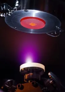
Like other physical and chemical vapour deposition methods, PLD must be performed in a low-pressure or vacuum chamber in deposition systems. The deposition process starts when a high-power laser (typically in the ultraviolet or infrared wavelengths) beam hits the target material. This causes the target’s molecules to break apart in a process called ablation, creating high-energy plasma known as an ablation plume.
The plasma plumes consist of positive ions of the target material and free electrons. As these ions meet the substrate, they settle on its surface in an atomic layer-by-layer growth process.
The physical, magnetic, and optical properties of PLD-grown thin films depend on the film’s structure – i.e., on the arrangement of atoms or ions in the coating material. Manipulating the material’s crystal structure allows the manufacturer to adjust the film’s properties.
PLD’s precision and flexibility make this technique an excellent choice when there is a need to grow thin films of complex materials, like buffer layers for microelectronics and optical devices. However, due to high costs and deposition scale limitations, other methods may be preferable in large area deposition.
Below, we will dive deeper into how the PLD process works, the applications of PLD in the coatings industry, and the comparative advantages and disadvantages of this thin film deposition method as contrasted with other deposition processes.
A Brief History of Pulsed Laser Deposition
PLD development began shortly after Maiman’s development of the ruby laser in 1960. In 1962, Breech and Cross first used a laser to vaporise solid material atoms. In 1965, Smith and Turner achieved the first successful deposition of thin films using a laser.
In those early years, PLD-deposited films could not compete with films produced by methods like a chemical deposition or molecular beam epitaxy. During the 1980s, technological developments such as excimer lasers facilitated better results from laser-based deposition.
Building upon these earlier developments, pulsed laser deposition took a leap forward in 1987 when researchers successfully used PLD to deposit a high-quality film of yttrium barium copper oxide (YBCO), a crystalline compound that exhibits high-temperature superconductivity. Since then, PLD has gained recognition as an effective method of producing superior-quality crystalline coatings, superconducting films with complex stoichiometry, oxide films like ITO (indium tin oxide), metallic multilayers, and nitride films. These materials are commonly used for coated conductor applications, like micro electromechanical systems (MEMS), and many more.
Laser technology advanced further in the 1990s with the development of high-repetition rate and short-pulse lasers. This technological progress enabled PLD to evolve into the ultra-precise, competitive thin film deposition method, particularly for coatings with complex stoichiometry.
Laser Absorption and Laser Ablation
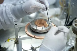
The laser beam interacts with the target surface fixed in place by a target holder, creating a plasma plume. The plume consists of molecules, atoms, ions, electrons, and, in some cases, larger particles of ablated material. The target holder is typically rotatable, utilizing planetary gearsets to enable rotation of different targets into position, and to ensure even and efficient use of targets.
The highly energetic plasma moves away from the target surface and eventually collides with the substrate, forming a film of the target material. In order to deposit pure films, the target material must reach the substrate without interacting with other particles in the deposition chamber. If the vacuum level isn’t sufficient, the mean free path within the deposition chamber will be short, and the probability of target material interacting with atmosphere increases sharply.
Plasma Dynamics
The laser pulse length and laser wavelength of the electromagnetic radiation from the laser influence the excitation process in the PLD chamber. A short-pulse laser will elicit electrostatic ablation based on electronic excitation. Longer laser pulses lead to higher temperatures and a mechanism known as thermal ablation, in which the ablation plume absorbs much of the laser energy.
Deposition of the Ablation Material
As the extracted target material evaporates, it collides with the substrate, resulting in film growth. Only a fraction of the bulk material’s top surface converts into a plume with each laser pulse. This results in exceptionally high-quality films with a superior level of control over film parameters, at the cost of deposition rate.
Nucleation (Growth of the Thin Film on the Substrate)
Under optimal conditions, pulsed laser deposition creates a deposited film layer of highly repeatable composition, structure, and of uniform thickness. The operators can control the environment in the deposition chamber, such as the gas composition and pressure, to fine-tune film growth.
PLD can occur in different gas environments and under varying background pressure. For example, in order to grow metal oxide films, oxygen gas is added to the process chamber to ensure enough oxygen is present to bind with the metallic target material. Using the same principle, nitride film deposition typically takes place with nitrogen gas added to the process chamber.
Factors Affecting Pulsed Laser Deposition
Thickness, composition, crystallinity, roughness, uniformity, and other deposited film properties depend on the parameters in the PLD deposition chamber, like gas pressure, laser fluence (fluence is the energy delivered per unit area by the laser), and laser pulse repetition rate.
The deposited material amount per unit of the surface area also depends on the substrate distance from the target, or throw distance. A greater throw distance results in less deposited material but will typically produce a higher-quality film.
Background gas pressure influences film growth rate, stoichiometry, and crystallinity. More gas leads to lower kinetic energies of the target material particles and enables the creation of high-crystallinity films. Conversely, low gas pressure allows relatively high-energy particles that may deposit too fast to form a crystalline structure.
Crystallinity also depends on the substrate temperature and the chamber’s thermal equilibrium. A heated substrate aids the creation of crystalline films, while lower surface temperatures may cause an amorphous film structure.
Advantages and Disadvantages of Pulsed Laser Deposition
PLD is the preferred method in many applications of thin films thanks to its unique advantages, such as:
- Delicateness. PLD can be performed at low temperatures and short test periods. The PLD process is flexible and compatible with many target and substrate materials that can’t tolerate high heat that is present in other physical vapour deposition techniques.
- Precision. PLD enables the preparation of highly uniform, multi-component films with an excellent degree of control over the stoichiometry of the deposited film.
- Sustainability. The PLD technique utilises high-energy UV or IR lasers for generating plasma. It is an energy-efficient method of producing thin films.
However, PLD also has some drawbacks. The PLD technique has a slow average rate of deposition and may be less suitable for covering large substrate areas compared to other methods.
Additionally, depending on the material and deposition parameters, small particles of the already-deposited film may sputter when bombarded by additional high-energy particles in the laser-induced process. This occurrence may compromise film quality.
Overall, PLD’s costs and currently available deposition scale make the method best suited for high-tech applications like sensor technology, optical technology, and microelectronics.
Difference Between Pulsed Laser Deposition and Thermal Evaporation
Although both PLD and thermal evaporation are physical vapour deposition methods, several key differences exist between the two techniques.
While PLD uses UV or IR light as an energy source, thermal evaporation produces thin coatings of vaporised material under high temperatures in a high-vacuum environment. Thermal evaporation deposition is straightforward, cost-effective, and suitable for large-scale applications like solar cells, semiconductors, and ultra-thin metal plating for consumer packaging.
Although thermal evaporation can also produce high-purity metallic and nonmetallic films, PLD is the method of choice when manufacturers need to grow thin films of complex composition, stoichiometry, and structure, like organic-inorganic hybrids, and metal oxides and nitrides.
Pulsed Laser Deposition Applications
PLD’s sensitive process control and comparatively high costs make this technique suitable for a range of applications that require ultra-high-quality complex films.
Examples of PLD uses include:
- Diamond-like coatings for optics and other high-precision applications
- Superconducting films for Josephson junction and quantum computing applications
- Single-walled nanotubes for sensors, biomedical devices, and wearable electronics
- Graded coatings for corrosion and thermal barriers
- Biocompatible coatings for medical applications
As advanced excimer laser devlopment continues, PLD will likely gain a larger foothold in various industries thanks to its ability to produce highly controlled, ultra-pure thin films in on- and off-axis deposition.
Final Thoughts
Pulsed laser deposition is a highly accurate method for producing thin films of superior quality, especially in applications that require coatings of complex materials with precise stoichiometry. PLD uses a straightforward laser-based process that allows for exceptional control over film properties.
PLD’s suitability for creating crystalline films makes this technique highly promising in the development of future applications that require superconductive or diamond-hard coatings.
Would you like to learn more about different coating techniques? Browse other articles by Korvus Technology, a producer of advanced thin film deposition systems.
References
[1] Greer, J.A. (2014). History and current status of commercial pulsed laser deposition equipment. Journal of PhysicsD: Applied Physics, 47(3).
[2] Albu, D.F., J. Lungu, G. Popescu-Pelin, C.N. Mihailescu, G. Socol, A. Georgescu, M. Socol, A. Banica, V. Ciupina, & I.N. Mihailescu. (2022). Thin film fabrication by pulsed laser deposition from TiO2 targets in O2, N2, He, or Ar for dye-sensitized solar cells. Coatings, 12(3), 293.
[3] Martínez-Landeros, V.H., N. Hernandez-Como, G. Gutierrez-Heredia, M.A. Quevedo-Lopez, & F.S. Aguirre-Tostado. (2019). Structural, chemical and electrical properties of CdS thin films fabricated by pulsed laser deposition using varying background gas pressure. Thin Solid Films, 682, 24-28.
[4] Ojeda, A., M. Dobeli, & T. Lippert. (2018). Influence of plume properties on thin film composition in pulsed laser deposition. Advanced Materials Interfaces, 5(18).
[5] Wang, H., Y. Wu, M. Ma, S. Dong, Q. Li, J. Du, H. Zhang, & Q. Xu. (2019). Pulsed laser deposition of CsPbBr3 films for application in Perovskite solar cells. ACS Applied Energy Materials, 2(3), 2305–2312.