An Introduction to hiPIMS Technology
From manufacturing shiny consumer electronics like the latest iPhone to solar cells, thin film deposition is a vital technology for the 21st century and beyond. HiPIMS coating properties represent a new generation of film deposition techniques for a variety of applications.
Short for High Power Impulse Magnetron Sputtering, HiPIMS is a state-of-the-art technology that allows for the superior application of thin film coatings. This coating technology is ringing in a new era of thin film production thanks to a reliable, multi-functional power supply and rapid arc-handling.
Conventional magnetron sputtering is not a new technology. Though magnetron sputtering processes have been around since the middle of the 19th century, the sputtering technology didn’t become a commercially viable solution until the 1970s. By contrast, HiPIMS reflects an advanced leap in the sputtering process, and is still advancing.
This article serves as an introduction to help familiarise readers with how HiPIMS works, its numerous advantages, and how it can be applied across a variety of products and industries.
How HiPIMS Works
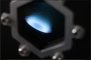
High Power Impulse Magnetron Sputtering uses high peak power voltage, short duration bursts of energy to coat target materials in a process referred to as ionized physical vapour deposition. The high peak power density and higher plasma density combined with the compressed “duty time” allows for denser, harder, and smoother coatings without overheating the target material or equipment for temperature-sensitive substrates. Process stability is maintained as a result of a low average cathode power.
Another key benefit of HiPIMS is that the improved thin films coating technology provides a more uniform application. From a practical standpoint, the HiPIMS process expands applications on substrate surface types that have more complex shapes.
The high power pulses associated with HiPIMS produce ionized atoms with higher energy levels than direct current magnetron sputtering. The result is a high-density plasma that yields up to a 90% increase in sputtered target material.
An overview of sputtering thin film processing goes something like this:
- Coating materials are set on a magnetron in solid form (referred to as a target).
- The chamber backfills with a process gas (usually argon, but also nitrogen or oxygen).
- The magnetron has a negative electrical potential applied to it.
- The electrical potential causes the acceleration of free electrons and a collision with the process gas atom.
- The gas atom is then stripped of the electron, which results in the creation of a positively charged process gas ion.
This ion then accelerates to the magnetron, carrying enough energy to sputter the material, also referred to as “knocking off.”
The sputtered material then collects on the substrate’s surface.
HiPIMS is not necessarily a replacement for traditional magnetron sputtering. Instead, the two processes complement each other, where a HiPIMS power supply and a DC power supply are added to existing sputtering systems.

Advantages of HiPIMS Technology
Unlike other seemingly disruptive technologies, the HiPIMS technique can be applied to conventional sputtering processes with minimal modifications required.
Advantages of HiPIMS technology include:
- Improved film density and adhesion
- Better film uniformity
- Increased control over film thickness and structure
- Reduced substrate damage
- Greater efficiency and cost-effectiveness
- Lower environmental impact
As HiPIMS technology becomes prevalent in practical applications, it is increasingly studied and applied in various industrial conditions. It’s already been shown that HiPIMS yields dense plasma at an order of magnitude higher than conventional techniques. High plasma density, in turn, facilitates more favourable growth conditions for film structures.
Because HiPIMS use ions rather than atoms for film growth, properties of thin films can be enhanced and built to more exacting standards. These deposited films can range in thickness from an atomic layer to several micrometres. In addition to practical applications, it’s also been suggested that HiPIMS technology is more favourable for the environment.
Applications of HiPIMS Technology
HiPIMS technology has a potentially infinite array of possibilities. From advancing medical devices to improving aesthetics and textures, HiPIMS is literally changing the face of consumer products, medical devices, and more.
The most common existing and emerging applications of HiPIMS technology include:
Electronics: HiPIMS can be leveraged to improve performance, functionality, efficiency, and the aesthetics of electronic devices.
Optics: Eyewear utilising plastic material is lightweight, comfortable, and durable. Unfortunately, these plastic lenses scratch easily and become discoloured. PVD processes utilising this technology can vastly improve optics.
Energy: Solar panels and other energy-generating applications can benefit from this new technology.
Aerospace and transportation: Companies like Bosch are applying High Power Impulse Magnetron Sputtering coating properties for combustion engines.
Other emerging applications: From food packaging to jewellery, various products can benefit from this technology.
Final Thoughts
HiPIMS is becoming the preferred coating technology across applications, from research to cutting-edge technologists seeking coatings that are denser, harder, and smoother than conventional coatings technology allows.
As these applications become more demanding HiPIMS technology will increasingly grow in importance in the area of advancing thin film deposition. Contact us to learn more about Korvus’ HEX sputtering system and its FISSION magnetron source’s compatibility with HiPIMS power supplies..
References:
[1] Gerhard Eichenhofer, et al. (2017). “Industrial Use of HiPIMS up to Now and a Glance into the Future, A Review by a Manufacturer Introduction of the hiP-V hiPlus Technology” Universal Journal of Physics and Application 11(3): 73-79.
[2] “Tutorial: Reactive high power impulse magnetron sputtering (R-HiPIMS),” Journal of Applied Physics, Volume 121, Issue 17 (2017).
[3] Steffen Drache, et al. (2013). “Time-resolved Langmuir probe investigation of hybrid power impulse magnetron sputtering discharges,” Vacuum, Volume 90, Pages 176-181.
[4] Zdenek Hubicka, et al. (2020) “Hardware and power management for high power impulse magnetron sputtering,” Fundamentals, Technologies, Challenges and Applications,” Pages 49-80.
[5] Mattias Samuelsson, “Fundamental aspects of HiPIMS under industrial conditions,” Linkoping University, Dissertation No. 1461 (2012).