Ion Beam Sputtering: How Does It Work?
Do you want to learn more about ion beam sputtering and the thin film deposition process? Ion beam deposition is necessary for dozens of industries and products that make our everyday lives easier, including optics and electronics.
At Korvus Technology, we’re proud to be the preferred choice in the UK for thin film deposition systems, including our cutting-edge HEX Series. Over 25 universities, research labs, and organisations trust our company to provide high-quality films and advanced deposition systems.
This article will explain all about ion beam deposition vs sputtering, including basic information, how the processes work, advantages, drawbacks, and modern applications.
What Is Ion Beam Sputtering?
Ion beam sputter deposition (IBSD) is a subcategory of physical vapour deposition. It offers unique advantages over its sibling processes, such as magnetron sputtering, ion plating, evaporation, and pulsed laser deposition.
Traditionally, manufacturers use ion energy of about 1000 eV and Ar ions with a fixed geometry when performing ion beam sputter deposition.
When a particle travels and encounters a target, both collide and transfer their momentum and energy. While several processes can result from ion-solid interaction like the one we just described, three are critical for ion beam deposition: implantation, sputtering, and scattering.
Ion beam deposition is an essential process for many organisations because it allows for a high level of customisation and imparts many valuable film properties. For example, IBS creates a dense structure and film thickness, superior adhesion, increased purity, fewer defects, and ideal target composition. The ion beam is highly collimated, and the ions possess equal energy, allowing for independent control over film stoichiometry and film thickness when deposited.
These benefits are particularly noticeable compared to other physical vapour deposition processes, such as magnetron sputtering, RF sputtering, or evaporated coatings.
Ion Beam Deposition Processes: How It Works
We mentioned that IBS is a form of physical vapour deposition (PVD), which is different from chemical vapour deposition (CVD). Both processes cause the growth of thin films on the target material substrate. However, PVD uses physical means to grow the film, while CVD uses chemical reactions.
During physical vapour deposition, thin film growth occurs upon the substrate surface in a vacuum chamber using metallic or dielectric film. When manufacturers perform ion beam deposition (IBD), they sputter low-energy ions and a broad-beam ion source with high voltage acceleration at the target material. As this occurs, the ions strike against the target substrate, expelling atoms and molecules.
Next, the thin film layer forms a tight bond and begins to condense on the surface of the target material, with both sputtered target material and scattered incident ions being deposited. Manufacturers can further enhance their control during the IBD process by adding a second gridded ion source (i.e., an ion gun) aimed at the substrate.
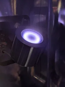
IBS requires a deposition system with the correct vacuum chamber to allow for the sputtering process and resulting condensation and growth of the IBS coating. The size of each IBS system varies based on the specific industry application. However, the HEX Series we manufacture here at Korvus Technology allows for excellent precision and supports a wide range of deposition techniques, including ion beam sputtering.
Ion Beam Sputtering vs Magnetron Sputtering
We just explained how an IBD system undergoes ion beam sputtering to provide control over the chemical and mechanical properties of a thin film. Sputtering processes aren’t just for ion beams, though. Magnetron sputtering is another form of PVD; however, it’s different from ion beam sputter deposition.
Here’s how it works: A magnetic field confines the target and substrate while an inert gas becomes fully ionised in plasma between them. Positive ions accelerate rapidly towards the sputtered target material, which is biased. Manufacturers can use magnetron sputtering at lower pressures, as magnets can stabilise changes.
Magnetron sputtering and ion beam sputter deposition have one significant difference: With IBSD, the target material and substrate do not have any plasma between them. Instead, the ion source securely houses the plasma. Furthermore, ion beam deposition doesn’t have target bias, meaning manufacturers can use sensitive, conductive, and non-conductive substrate/target material.
Another difference between these sputtering processes is the level of independent control offered by ion beam sputtering. You can set specific parameters for the target sputtering rate (deposition rate), angle of incidence, ion energy, ion current density, and ion flux. The resulting ion beam sputtering coating is smooth, dense, and deposited tightly to the substrate.
Advantages and Disadvantages of Ion Beam Sputtering
Ion beam sputtering deposition provides manufacturers and countless industries with several advantages, including optimal energy bonding properties, versatility, precision control, and uniformity.
Energy Bonding
Ion beam sputter coating uses energy bonding at around 100 times higher than vacuum coating. Even after surface deposition, enough kinetic energy remains to ensure superior quality and a strong bond.
Uniformity
Most ion beam sputtering originates from a relatively large target surface, providing stronger uniformity. Furthermore, it allows for greater composition and target material flexibility than other forms of sputtering.
Precise Control
During ion beam deposition, manufacturers can focus and scan the ion beam precisely, and the sputtering rate, energy, and current density can undergo minute adjustments for optimal conditions.
Of course, despite the superior control and precision that ion beam sputtering allows, it also has some limitations. For example, if you have a large surface and want a film of uniform thickness, ion beam sputtering may not be the best choice. Even with dual ion beam sputtering, the target area isn’t large enough, resulting in a low deposition rate.
Applications for Ion Beam Sputtering and Ion-assisted Deposition
Ion beam sputtering creates unique opportunities for challenging applications. Applying ion sources to film coatings can also increase energy and mobility before nucleation.
Common applications for ionbeam sputtering include precision optics, nitride films, and semiconductor production. For example, researchers have been studying the effect of bombarding certain films with O2+ and Ar+ during deposition, resulting in changes to film stoichiometry, including increased density, modifications to the crystal film structure, and decreased water permeability.
Furthermore, ion beam sputtering is vital for applications like laser bar coating, lenses, and gyroscopes. Many manufacturers use an ion source during the deposition process to gain precise control over the removal of surface layers down to an atomic scale. Furthermore, ion beam sputtering helps create a clean surface in field electron microscopy, low-energy electron diffraction, and Auger analysis.
With an ion beam that uses a sharp edge, manufacturers can perform damage-free cuts of thick films, like ion beam slope cutting. The process is invaluable for optical elements, including dispersive mirrors, glasses, insulators, and lenses.
However, arguably the most widespread application of IBS is the deposition of thin films onto a chosen substrate. The deposition process is suitable for large-scale or small-scale substrates, such as microelectronics.
Final Thoughts
Ion beam deposition and thin films are indispensable for modern-day technology. With numerous applications, precise levels of control, and the creation of smooth, dense films, ion beam sputtering is one of the best physical vapour deposition techniques.
At Korvus Technology, we want our clients to be well informed about deposition and how the process works, including physical and chemical vapour techniques. If you are considering the use of a sputtering system for your own projects, our HEX Series deposition system is trusted by organisations worldwide, who appreciate its versatility, advanced technology, and extraordinary workmanship. If you have more questions about ion beam sputtering, keep reading the Korvus Technology blog or reach out for a quote using our convenient online form.
References
1. Abdelrahman, M. M. (2015). Study of plasma and ion beam sputtering processes. Journal of Physical Science and Application, 5(2). https://doi.org/10.17265/2159-5348/2015.02.007
2. Behrisch, R., (Ed.). (2013). Sputtering by particle bombardment I: Physical sputtering of single-element solids. Springer. ISBN 978–3662308882.
3. Bundesmann, C., & Neumann, H. (2018). Tutorial: The systematics of ion beam sputtering for deposition of thin films with tailored properties. Journal of Applied Physics, 124(23), 231102. https://doi.org/10.1063/1.5054046
4. Chen, Y., Hahner, D., Trubetskov, M., & Schramyere, S. (2020). Comparison of magnetron sputtering and ion beam sputtering on dispersive mirrors. Applied Physics B, 126(5), 82. https://doi.org/10.1007/s00340-020-07431-6
5. Forrester, A. T. (1988). Large ion beams: Fundamentals of generation and propagation. Wiley-VCH. ISBN 978–0471625575.
6. Seshan, K., & Schepis, D. (2018). Handbook of thin film deposition. Science Direct. Elsevier, William Andrew. Retrieved August 25, 2022, from https://www.sciencedirect.com/book/9781437778731/handbook-of-thin-film-deposition#book-info.