Shaping Light With Deposition: An Introduction to Optical Thin Films
Modern physical vapour deposition (PVD) techniques, such as electron beam evaporation and sputtering, allow for the creation of optical thin film coatings. Optical coatings enhance the strength and reflective capabilities of many everyday products, including windows, eyeglasses, and camera lenses.
Thin Film Deposition Techniques
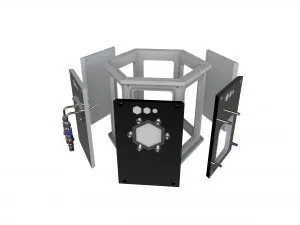
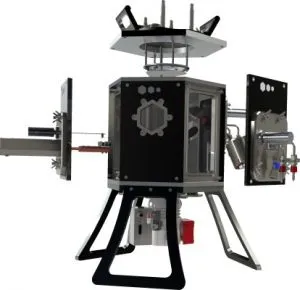
State-of-the-art PVD machines, like the Korvus Technology HEX benchtop coating system, have made it possible for researchers, manufacturers, and students to create thin films using various methods. One such physical vapour deposition procedure involves heating a solid material at high temperatures using an electron or thermal evaporation crucible and creating a thin layer on a target substrate.
In contrast, chemical vapour deposition (CVD) uses volatile substances to either react with or dissolve the target material to achieve the desired optical properties. A user can deploy CVD by utilising an ion source in a flow-controlled reaction chamber. The microfabrication of circuit boards relies on the CVD method to deposit materials like polycrystalline and epitaxial.
The atomic layer deposition technique (ALD) is a method many researchers consider an alternative form of CVD. This method requires precise fine-tuning of the target material’s atomic makeup. Many industries use this precise deposition method to optimise film thickness and spectral characteristics.
Still, PVD allows manufacturers and researchers to deploy multiple techniques to achieve their desired results. For example, electron beam (e-beam evaporation) deposition enables users to evaporate metals with high melting points, like aluminium, without cracking the substrate. Sputtering and pulsed laser deposition can also create thin films on fragile glass substrates.
While all the above methods can produce a protective optical coating, PVD may be the most reliable choice. For instance, ion-assisted deposition effectively creates high-durability, anti-reflection coatings for corrective lenses and solar cells. Sputtering also uses a low-temperature vacuum chamber to reduce disruptive thermal noise during deposition. Some sputtering techniques have drawbacks however, potential problems like target poisoning can occur which can affect magnetron’s efficiency.
There are many ways to enhance the thickness and mechanical properties of an optical film deposit with PVD and CVD. The fabrication method you choose will depend on factors like your budget, the geometric surface of your substrate, and deposition time. User experience and accurate measurements are also important factors in achieving successfully deposited thin films.
Materials for Optical Thin Films
Dielectric materials can create single or multi-layer anti-reflective coatings for camera lenses, optical fibres, and other high-end photonic devices. These materials include high-density silicon dioxide film and barium strontium titanate (BST). Dielectric materials come in different thicknesses, but are usually hard.
Some dielectric optical thin films (particularly multi-layer dielectric film) can even provide a range of aesthetic enhancements through optical interference. Manufacturers can use these coatings to separate light in wavelengths, creating a gradient appearance.
Aluminium, titanium, gold, and crystalline niobium are popular metallic materials used for optical thin films. The guiding layer of these metallic materials typically has a higher refractive index than the substrate, allowing visible light to reflect and refract into the optical thin film.
Hybrid and novel materials, such as polyimide/silica, come in different thicknesses and film structure. Most hybrid materials have a thickness of 100 nm or less, which is also good for magnetism and catalysis applications.
Consider a few factors when choosing suitable materials for optical coatings. For example, Bragg mirror manufacturers may want dielectric materials for the most efficient anti-reflective coatings for lasers. On the other hand, metallic materials provide the highest refractive index rating and may be suitable for many biomedical applications.
Thin Film Deposition Process
Creating thin film coatings requires careful preparation of the substrate and the correct placement of optical components. For PVD methods, users can place the target thin film material at the bottom of the chamber and aim an ion gun or electron beam laser at the surface. The substrate should be directly above the heated material.
Other methods, such as the dip coating method, may require users to soak the substrate into a conformal coating before leaving it to dry.
The deposition procedure begins when evaporation or sputtering starts to target the material and create layers of thin films on the substrate. With magnetron sputtering, a magnetic field encompasses the electrons in the chamber, creating a plasma that sputters the deposition source. With the electron evaporation method, a laser fires electrons into the material, causing particles to form a deposit on the sample.
Some PVD machines have automated features that allow users to monitor and control the process through a computer or integrated control panel such as those manufactured by Korvus Technology.
Optical Thin Film Applications
Optical thin films have many applications in development, research, and consumer sectors.
Anti-reflective coatings reduce light interference and maximise visual acuity. Single-layer thin films are practical for lasers and solar cells. Multi-layer, anti-reflective thin films provide better broadband performance and are useful in the aerospace industry and telescopes.
Conversely, some optical devices like photovoltaic cells and lasers use high-reflective thin film coatings to optimise power consumption. They are also practical for mirrors or to create a “silvering” effect on some consumer products.
Optical filters can improve or enhance an image with powerful infrared transmission capabilities. Additionally, thin films have optical elements like quantum dots that can create beam splitters and robust coatings for laser systems.
A linear variable filter may be helpful for spectroscopic and analytical applications, allowing researchers to measure the transmittance of light over short wavelengths. Linear variable filters may continue to play a vital role in the emergence of other applications that rely on optical thin films.
Advancements and Challenges
Recent advancements in PVD and CVD techniques make optical thin films more accessible to manufacturers in the modern industry. Still, maximising stability and reducing the toxicity of thin film deposits pose challenges for researchers. As more technology advances in this field, answers may soon come to light.
Contact Korvus Technology Ltd online or explore the following articles to learn more about RF sputtering, the differences between PVD and CVD, and thin film interference.
References:
[1] Behera, Ajit, Review article: Chapter 13 – Nanocoatings for anticorrosion: An introduction. Corrosion Protection at the Nanoscale, Pages 227-243, 2020.
[2] Guglya, Aleksey, Review article: Chapter 4 – Ion-beam-assisted deposition of thin films. Emerging Applications of Nanoparticles and Architecture Nanostructures, Pages 95-119, 2018.
[3] Hirano, Takuya, Review article: Influence of aluminum interlayer on optical properties of very thin silver thin film. Surface and Coatings Technology, Volume 393, 15 July 2020.
[4] Wang, Fuzhen, Review article: Chapter 18 – Applications in thermoelectric thin films. Modern Ion Plating Technology, Pages 459-473, 2023.