Sample Preparation
Thin film on substrate for analysis
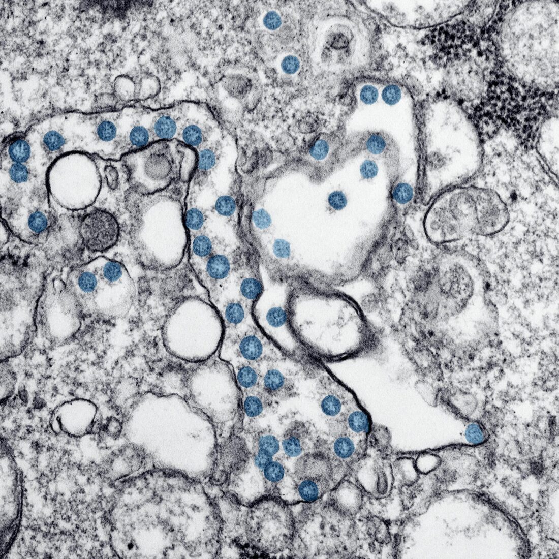
In microscopy, so called electron microscopes, are used to offer resolutions and magnifications far higher than traditional optical microscopes due to the inherent short wavelengths’ electrons offer compared to photons of visible light.
A key prerequisite to using an electron microscope is the development of a conductive layer on the surface of the sample. Many materials that may wish to be imaged via electron microscopy are non-conducting (such as biological samples and organic polymers), which means that as the electron beam necessary for imaging passes through the sample, a charge can build up on the sample and prevent any transmission of electrons through the sample. To combat this, a thin layer (a few nm) of conductive material must be deposited on the surface to avoid this charge buildup.
The most common and simple way to do this is via PVD and magnetron sputtering; in this process, the entire system is brought under vacuum, and a plasma is generated on the surface of a conductive target. A voltage is placed across the system, and charged ions in the plasma collide with the target, sputtering off pieces of material. The sputtered material moves across the chamber and condenses onto the sample in the form of a thin film.
Sample prep in this way is key to many breakthroughs, with SEM and TEM samples giving us insights into the inner workings of cells and other materials previously unattainable with traditional microscopy. At Korvus Technology, we have developed a compact, tabletop system that can assist with just this – The HEX-Mini is perfectly positioned to aid with any and all coatings, including microscopy sample preparation, while maintaining its integrity as an entry-level PVD option.
The HEX Mini
Benchtop Coater Ideal for Sample Preparation

Frequently Asked Questions
What role does PVD play in sample preparation ?
Physical Vapour Deposition (PVD) plays a crucial role in sample preparation, especially in materials science, nanotechnology, electronics, and surface analysis. It’s used to create thin, controlled coatings on samples to tailor their surface properties, electrical behaviour, optical performance, or structural compatibility for further study or integration into devices.
What are examples of PVD in Sample Preparation
XPS Sample: Depositing a thin Au or Ag film to prevent charge buildup on the surface and enhance signals
SEM Imaging: Sputter-coating non-conductive polymers with gold to allow for electron transfer
Solar Cell Study: Evaporating ITO, MoO₃, or Ag to form electrical contacts
Tribology Test: Coating samples with TiN or CrN to study wear and friction
Perovskite Devices: Using PVD to deposit electron/hole transport layers
Why is PVD used in SEM / TEM?
PVD is an essential tool for electron microscopy (SEM, TEM) when working with non-conductive samples as it allows for them to be imaged. A thin Au, Pt, or Cr deposited layer prevents charge build up on the surface which helps to enable clear imaging and gives some surface contrast. This technique is also used in nanoindentation or contact resistance testing.
How does PVD impact surface properties?
Alters surface conductivity, roughness, chemical reactivity, or wettability and prepares surfaces for:
Microscopy (e.g., SEM, TEM)
Spectroscopy (e.g., XPS, AES)
Adhesion enhancement for other coatings
What Functional thin films is PVD used for?
Deposits of metals, oxides, nitrides, or semiconductors on substrates can be used to prepare layers like:
Electrodes (e.g., Au, Pt, ITO)
Barrier or buffer layers (e.g., TiN, SiO₂)
Light-absorbing or active layers (e.g., Mo, VO₂)
These films help to enable functional testing in solar cells, sensors, MEMS, and more