Power electronics is an industry that is constantly evolving, and silicon carbide thin films are the latest technology driving that evolution. With their unique properties and performance, silicon carbide thin films have the potential to revolutionise many power electronic applications. This article will explore the properties, deposition methods, and potential applications of silicon carbide thin films in power electronics.
Silicon carbide, or SiC, is a compound of silicon and carbon known for its hardness and high thermal conductivity. SiC is commonly used to make cutting tools, abrasives, and refractory materials in high-temperature applications. SiC can also be deposited as a thin film on different substrates, creating a range of unique properties.
SiC is a semiconductor material with a wide bandgap of 3.2 eV, making it capable of operation at high temperatures and power levels. SiC is also chemically and thermally stable, which makes it resistant to chemical and thermal degradation. These properties result in the potential for much higher power density and efficiency at high frequencies.
The manufacturing process

Silicon carbide thin films are typically formed by chemical vapour deposition (CVD). This process allows for the deposition of thin films of SiC onto a substrate at a controlled rate. It is possible to deposit different types of SiC films, such as amorphous, polycrystalline, and crystalline, depending on the deposition process and deposition parameters.
In that sense, amorphous SiC is one of the most commonly used SiC thin films in power electronic applications. This film has a random arrangement of atoms and lacks the long-range order of crystalline SiC. Amorphous SiC thin films have a lower coefficient of thermal expansion compared to other materials, making them ideal for high-temperature applications.
How Are Silicon Carbide Thin Films Deposited?
There are different thin-film deposition systems that can be used to improve the quality of materials. In this section, we’ll take a look at some of the most common ways of creating silicon carbide films.
Physical Vapour Deposition (PVD)
PVD is a common vacuum deposition technique that involves using a physical process to deposit a thin film of a solid material onto a substrate. This can be done through several processes such as thermal and e-beam evaporation, along with a process known as sputtering.
Sputtering occurs through the bombardment of positively charged ions onto a target material which will then sputter off pieces of the target, causing them to move through the chamber and condense onto the substrate. Sputtering is an essential tool for PVD as it allows for the deposition of insulating and semiconducting materials such as SiC.
Polycrystalline SiC Thin Films
Polycrystalline SiC thin films are formed by depositing SiC on a substrate in a polycrystalline form. This process allows for the growth of SiC in a crystalline form with larger grains than amorphous SiC. Polycrystalline SiC thin films have higher electrical conductivity than amorphous SiC thin films and can be used in specific power electronic applications.
Crystalline SiC Thin Films on Silicon Substrate
Crystalline SiC thin films are formed by depositing SiC on a silicon substrate. This process results in the growth of single-crystalline SiC thin films, which have high electrical conductivity and mechanical strength. Crystalline SiC thin films are ideal for use in high-power and high-frequency applications, such as power amplifiers and high-frequency inverters.
What Are The Unique Properties?
Silicon carbide thin films exhibit high mechanical strength, making them ideal for use in harsh environments. SiC thin films have a high Young’s modulus, hardness, and stiffness compared to other materials, enabling them to withstand high mechanical stresses.
On the other hand, films using SiC exhibit excellent high-temperature performance, making them ideal for use in high-temperature applications. This is due to SiC being thermally stable and not being degraded at high temperatures, enabling devices to operate reliably in high-temperature environments.
Moreover, SiC thin films can be deposited with precise thickness and uniformity, enabling the fabrication of devices with excellent performance and reproducibility. SiC thin films can be deposited with a thickness as low as a few nanometres or as thick as several microns, depending on the deposition process and parameters.
Why Are they Revolutionising Power Electronics?
Here at Korvus Technology, we believe that crystalline SiC films can become one of the most important innovations in the field of electronics. Here are a few reasons why:
Improved Performance Of Power Devices Using SiC Thin Films
Silicon carbide thin films have unique properties that enable them to be incorporated into power electronic devices, resulting in improved performance. For example, SiC thin films exhibit high electrical conductivity and low on-state resistance, resulting in a significant reduction in power losses and increased device efficiency.
Reduced Power Losses And Increased Efficiency With SiC Thin Films
In terms of their electrical properties, SiC thin films exhibit low switching losses, which results in lower power consumption and increased efficiency in power electronic devices. SiC thin films allow for higher operating temperatures for devices, which reduces cooling requirements and simplifies thermal management.
Increased Reliability Of Devices With SiC Thin Films
Silicon carbide thin films have high mechanical strength and excellent high-temperature performance, resulting in increased reliability of power electronic devices. SiC thin films enable the fabrication of devices that can withstand harsh environments, resulting in a longer device lifetime and lower failure rates.
What Is The Future Of Silicon Carbide Thin Films In Power Electronics?
As we mentioned, SiC films are one of the most important electron beam evaporation applications as well as thin film deposition techniques. The current trend is to further improve the performance of power electronic devices by improving SiC thin films and exploring new application areas such as optoelectronics, sensors, and spintronics.
Future developments are likely to focus on further increasing the efficiency of SiC-based devices, reducing the costs of production, which means that this technology will continue to be a major player in the power electronics industry. The development of SiC-based technology continues to advance rapidly, and there are already multiple commercial products on the market utilising SiC thin films.
With the power electronics industry continuing to evolve and grow, it’s likely that there will be even more applications for SiC thin films in the future. Here are some of our predictions:
Potential For Further Power Device And System Integration Using SiC Thin Films
Silicon carbide thin films have the potential for further integration into power electronic devices and systems, enabling higher levels of integration and simplification of device design. SiC thin films can be integrated into a wide range of power electronic applications, including electric vehicles, renewable energy systems, and industrial applications.
Advancements In SiC Thin Film Technology For Even Better Performance And Reliability
The field of silicon carbide thin films is still rapidly evolving, with the potential for significant advancements in film quality, deposition process, and device performance. Researchers are continuously striving to improve the properties of SiC thin films, resulting in devices with higher efficiency and reliability.
Integration Into A Wide Range Of Power Electronic Applications
Silicon carbide thin films have the potential for integration into a wide range of power electronic applications, from microelectronics to high-power devices. SiC thin films offer unique material properties not found in other materials, enabling the fabrication of devices with higher efficiency, higher operating temperatures, and increased reliability.
Take Advantage of SiC Films With Korvus
Looking to apply a perfect thin-film coating to your building materials?
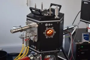
The HEX Series from Korvus Technology allows businesses to effectively deposit the right type of film on any substrate material. Our equipment is designed for precision and repeatability, allowing you to consistently produce high-quality coatings, no matter the application. You can choose from three types of deposition—sputtering, thermal evaporation, and e-beam evaporation—to suit your needs.
With the HEX Series by Korvus Technology, you get reliability, efficiency, and a low cost of ownership for all deposition processes that are critical in today’s electronics industry. We are also on hand to aid with any technical support that may arise throughout your work with our HEX series.
Visit our website now to learn more about how their HEX Series systems can help save costs while producing quality products!
References
[1] SVM International Inc., “Silicon Carbide Films,” SVM International Inc., 2021 [Online]. Available: https://svmi.com/service/silicon-carbide-films/. [Accessed: 06 May 2021].
[2] H. Liu, Y. Zhang, Y. Li, et al., “Synthesis of smooth amorphous thin films of silicon carbide by nanosecond pulsed laser deposition,” Applied Surface Science, vol. 486, pp. 549-556, 2019. https://link.springer.com/article/10.1007/s00339-022-05499-9
[3] M.-H. Huang and J.-Y. Chang, “Applications of SiC-Based Thin Films in Electronic and MEMS Devices,” in Silicon Carbide and Related Materials 2018, Springer International Publishing AG, 2018, pp. 825-829. https://www.intechopen.com/chapters/37838