Exploring the Process and Applications of Gold Sputtering
Gold sputtering is a method for adding a thin layer of gold to various surfaces, such as circuit boards, metal jewellery, or medical implants, through physical vapour deposition (PVD). The process involves exciting the atoms of the target or source material — typically, discs of solid gold or gold alloy — by bombarding them with high-energy ions in a vacuum chamber .
This causes the target material to start ejecting or “sputtering” a fine vapour of gold atoms or molecules, which lands on the target surface, also known as a substrate, in the form of a fine gold coating.
PVD gold sputtering often uses a direct current (DC) power source to excite the target material. DC sputtering is one of the simplest and least expensive sputtering methods. Alternative techniques include:
Thermal evaporation deposition: An electrical resistive heating element heats and evaporates the target material in a low-pressure environment.
Electron-beam vapour deposition: An electron beam heats the target material in a high vacuum environment, with the material eventually condensing on the substrate.
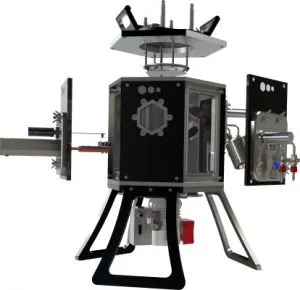
All types of gold sputtering processes require special sputtering equipment and controlled conditions.
Why Is Gold Used for Sputtering?
PVD gold sputtering is the go-to technique to apply coatings in the watch and jewellery industry. Sputtered gold films are exceptionally hard, durable, and corrosion resistant. They also resist tarnishing, maintain their sheen for a long time, and do not rub off easily due to repeated contact with skin or clothes. Gold sputtering also allows fine-grain control of where and how the gold vapour deposits to ensure a uniform gold coating or create custom patterns and shades like rose gold, which requires a specific mix of gold and copper as well as controlled oxidation of the free metal atoms in the sputtering process.
Due to the excellent conductivity of the metal, another major application of gold sputtering is coating circuit panels and electronic components in the electronics and semiconductor industries.
Gold sputtering is also invaluable in medicine and the life sciences, where it helps coat biomedical implants with radiopaque films that are visible in X-rays. Coating tissue samples in thin films also makes them visible under electron microscope scanning.
Another important advantage of PVD gold sputtering is that it is suitable even for materials with an extremely high melting point where traditional evaporation in a Knudsen cell or resistance evaporator would be challenging or impossible.
The Applications of Gold Sputtering
The addition of a PVD gold sputter coating helps improve the durability and performance of a wide range of metals and materials. As a result, gold sputtering has many applications across various industries.
What Industries Commonly Use Gold Sputtering?
Gold sputtering is commonly applied in the following industries:
- Watches and jewellery: Watches, rings, bracelets, necklaces, earrings
- Optics: Optical fibres, optical devices, lenses, projectors, digital cameras, security monitoring equipment, optical disc players, aerospace monitoring lenses
- Electronics and semiconductors: Circuit boards, data storage devices, flat panel displays
- Energy: Photovoltaics, solar cells, batteries
- Home and decorative: Taps, fixtures, cookware
- Medicine and life sciences: Medical and dental implants, coated specimens for electron microscope scanning
- Architecture and construction: Energy-efficient anti-reflexive coating for windows and glass
What Materials Can Be Coated With Gold Using Sputtering?
PVD gold sputtering coatings are compatible with a wide range of materials, including semiconductor materials, architectural glass, and valuable metals.
However, gold is not ideal for sputtering materials that will undergo high-magnification imaging. Due to its high secondary electron yield, gold tends to sputter rapidly, but the downside is that the coating structure contains large islands or grains that will be visible at high magnifications. That makes gold sputtering better suited to imaging at low magnifications, typically under 5000×, where the coating structure will not interfere with the structural details of the material surface.
The Role in Semiconductor Production
PVD gold sputtering is often used on circuit chips, boards, and other components in the semiconductor industry. This is largely due to the metal’s excellent electrical and thermal conductivity and the possibility of applying a thin layer of single-atom gold coating with extreme purity.
Semiconductor components have extremely high technical production requirements — more so than other applications of gold sputtering such as solar cells or flat-panel displays. The sputtering targets must be completely free of even trace impurities, as they can render the final product unusable.
Gold Sputtering vs Other Deposition Techniques
Coating materials with sputtered gold through PVD is different from gold plating and gold filling.
The PVD process involves applying a gold film in a high-energy plasma environment. The resulting coating provides a harder, stronger, and more durable surface bonding than either gold plating or gold filing. It is also easier to control the colour of the coated surface with PVD.
Gold plating involves an application of gold coating through electroplating in a chemical bath, in which an electrical charge is applied to the target surface to attract and bond the gold particles from the sputtering targets. The process is simple and relatively inexpensive but results in a softer and less durable coating. The chemical processes involved are also not environmentally friendly.
Gold filling uses high temperature and pressure to bond gold to metal mechanically. It produces a thicker coating than both gold plating and the PVD process and is usually more expensive because it requires greater quantities of the source metal.
Final Thoughts
The deposition of gold through sputtering has many benefits and applications across various fields. Gold-coated metal and other materials are common in the watch and jewellery, optics, semiconductor, electronics, medical, and energy industries.
That said, it is important to keep in mind that this is just one subtype of physical vapour deposition. Depending on the intended purpose, target substrate, and budget for the project, some of the other sputtering methods may be more appropriate.
References
[1] M. W. Thompson (1968). The energy spectrum of ejected atoms during the high energy sputtering of gold, The Philosophical Magazine: A Journal of Theoretical Experimental and Applied Physics, 18:152, 377-414. DOI: 10.1080/14786436808227358.
[2] M. Rabeeh, T. Hanas (2022). Enhancing biointerfacial properties of porous pure iron by gold sputtering for degradable implant applications, Materials Today Communications, 31, 103492. DOI: 10.1016/j.mtcomm.2022.103492.
[3] K. Tai, T. J. Houlahan Jr., J. G. Eden & S. J. Dillon (2013). Integration of microplasma with transmission electron microscopy: Real-time observation of gold sputtering and island formation, Scientific Reports, 3, 1325. DOI: 10.1038/srep01325.
[4] M. Sun, F. Zhang, Z. Tong, G. Sheng, Y. Chen, Y. Zhao, Y. Chen, S. Zhou, G. Liu & Y. Tian, H. Yu (2010). A gold-sputtered carbon paper as an anode for improved electricity generation from a microbial fuel cell inoculated with Shewanella oneidensis MR-1, Biosensors and Bioelectronics, 26:2, 338-343. DOI: 10.1016/j.bios.2010.08.010.