Thin-Film Solar Cells

THE HEX SERIES

Thin-Film Technologies for Solar Cells

Despite having dominated the solar-cell market since its beginning, crystalline Si solar cells are now being challenged by maturing thin-film technologies that offer cheaper alternatives at ever-improving efficiencies. Three of the main thin-film technologies disrupting the industry are:

  • Perovskites
  • Cadmium Telluride (CdTe)
  • Copper Indium Gallium Diselenide (CIGS)

All of these thin-film photovoltaic materials can be deposited by vacuum-based vapour deposition methods, like evaporation and sputtering, to produce high-quality films. Other layers within solar-cell architectures, such as transparent conducting oxides (TCOs), anti-reflection coatings and electrical contacts, can likewise be deposited by these methods. The high modularity of the HEX series, with the choice of FISSION, ORCA and TAU sources, provides materials researchers with an adaptable physical vapour deposition (PVD) platform that can be configured and altered to suit their solar-cell application needs. Please get in contact at sales@korvustech.com now to discuss your requirements and get a full system configuration that satisfies your research needs.

THE HEX SERIES

Perovskite Thin Films For Solar Cells

Perovskite thin films are the new kid on the block when it comes to solar-cell technologies, having surpassed the 20 % cell efficiency barrier in 2014. Thin-film perovskite solar cells are now producing efficiencies of 27.0 %, almost rivalling the best-performing Si cells (27.8 %). They have rapidly overtaken other 3rd-generation photovoltaic technologies, including quantum dot and organic solar cells, to become a key focus for many materials research laboratories that are keen to harness their desirable attributes.

Perovskites are a class of compounds with a specific crystal structure based upon the mineral perovskite, CaTiO3. Due to the wide range of suitable ions that can be substituted into the perovskite crystal structure, perovskites have a high degree of tunability and can have their properties adjusted for many optoelectronic applications, including photovoltaic devices.

Along with other thin-film solar cell technologies, perovskites provide cost advantages compared to Si cells due to the reduced amount of material needed to fabricate the photovoltaic cell as well as being able to unlock flexible device applications such as wearable electronics.

At Korvus Technology, we have over 20 years of experience working on PVD methods and have supported researchers in the perovskite field through our highly modular HEX series of PVD equipment. Our tools and sources provide a wide range of PVD methods applicable to the deposition of thin-film perovskites.

FISSION- Magnetron Sputtering Source

Magnetron Sputtering Scource
Designed for 2″, 3″ and 4″ diameter targets, the sputter sources are equipped with SmCo magnets and accept targets with thickness ranging from 0.5 to 6mm of non-magnetic materials and up to 1mm for magnetic materials. The most flexible source, the FISSION can be paired with DC, RF, HiPIMS, Pulsed-DC and more…

ORCA - Low Temperature Evaporation

low temperature evaporation
The ORCA organic deposition source is designed to operate between 50 and 600 C to allow sensitive organic materials to be evaporated with precise control. This source can also be used to evaporate low-temperature metals such as Lithium, and pairs well with the glovebox integration of the HEX Series.

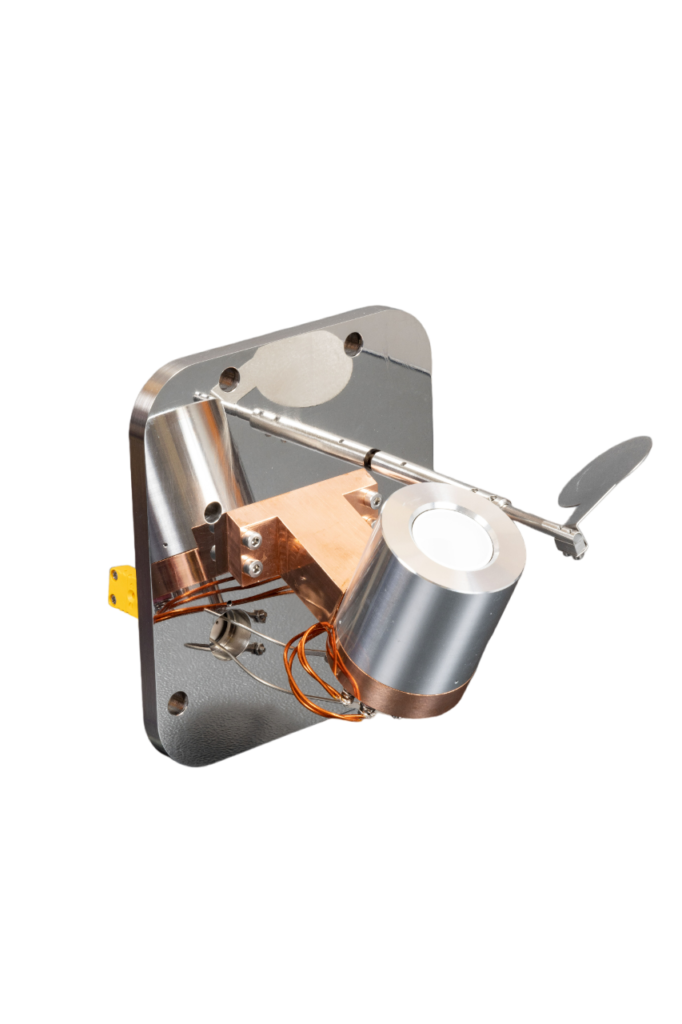
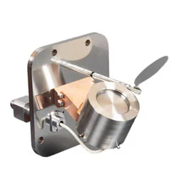
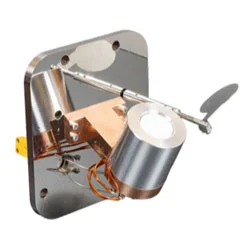
TAU - Electron Beam Evaporation

electron beam evaporation
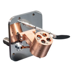
Our high-accuracy (sub-monolayer) mini E-beam evaporators are ideal for ultra-thin film deposition of high-temperature metals with reliable process control. Material can be evaporated from rods or material held in a crucible. Our novel design allows the material to be co-deposited from four individual pockets.

Frequently Asked Questions

A perovskite in PVD refers to perovskite materials that are deposited onto substrates using Physical Vapour Deposition techniques, such as evaporation or sputtering. This method is popular in the production of perovskite solar cells because it offers high control over the material properties, film quality, and scalability for large-area production. Despite the promise, challenges like moisture sensitivity, film uniformity, and toxicity (for lead-based perovskites) remain areas of ongoing research.

Physical Vapour Deposition (PVD) is a crucial tool in researching perovskites, particularly in the development of perovskite solar cells and other optoelectronic devices. PVD allows researchers to precisely control the deposition of perovskite materials, which is important for understanding their properties, optimizing their performance, and investigating new perovskite compositions and structures.

In perovskite research using PVD, several coatings are deposited to enhance the performance, stability, and efficiency of perovskite-based devices, particularly solar cells. These coatings include electron transport layers (ETLs), hole transport layers (HTLs), electrode layers, the active perovskite layer itself, and buffer/passivation layers. Each of these coatings plays a vital role in charge transport, device stability, and efficiency, and PVD techniques like sputtering and evaporation allow researchers to precisely control the deposition of these materials for optimal device performance.

Moisture sensitivity and the need for proper encapsulation.

Achieving correct stoichiometry and avoiding defects in perovskite films.

Controlling crystallization and film morphology for better charge transport.

Interface quality between the perovskite and other layers (e.g., ETL, HTL).

Scalability challenges when moving from lab-scale to large-area deposition.

Managing precursor materials and ensuring proper reaction for uniform perovskite formation.

Achieving uniform film thickness and consistent quality.

Environmental concerns related to lead-based perovskites.

Thermal degradation and the need for long-term stability.

By carefully addressing these challenges, researchers can optimize PVD processes for high-performance and long-lasting perovskite-based devices.

For perovskite research, the system will need to be connected to a glovebox so as to avoid contamination from a non-inert atmosphere. A suitable deposition tool such as a thermal evaporation or sputtering source would also be needed. 

There are other concerns depending on the type of perovskite and other materials that may be deposited in the chamber so for a full system configuration, please get in contact at sales@korvustech.com now.